In the intricate world of microelectronics manufacturing, photomasks and wafers play pivotal roles, yet they serve distinct purposes within the broader production process. Understanding the fundamental differences between these two critical components is essential to appreciating the complexities of modern semiconductor fabrication.
What is a Photomask?
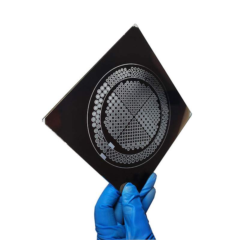
A photomask, also known as a light mask, photolithographic mask, or simply a mask, is a graphic transfer tool used in microelectronics and microfabrication technologies. It functions as a master template, carrying the intricate design patterns and intellectual property information necessary to produce intricate structures on wafers. Essentially, a photomask serves as a "blueprint" for the circuit patterns that will be etched onto silicon wafers during the photolithography process.
Key Features of Photomasks:
Material Composition: Photomasks are typically constructed on a transparent substrate, such as quartz glass, with a layer of metal chromium and a photosensitive film coated on top. This combination creates a high-resolution, light-sensitive surface capable of precisely transmitting or blocking light during exposure.
Function: They function similarly to the "negatives" used in traditional photography, transferring the designed patterns onto wafers during the photolithography step.
Applications: Photomasks are indispensable in various microfabrication technologies, including integrated circuits (ICs), flat panel displays (FPDs), printed circuit boards (PCBs), and microelectromechanical systems (MEMS).
What is a Wafer?
A wafer, on the other hand, is a thin slice of semiconductor material, primarily silicon, used as a base for the creation of integrated circuits and other microelectronic devices. During the manufacturing process, wafers undergo numerous steps, including cleaning, oxidation, photolithography, doping, etching, and deposition, to create the intricate circuitry required for electronic devices.
Key Features of Wafers:
Material: Wafers are made from high-purity silicon, which is a semiconductor material with unique electrical properties that make it ideal for microelectronics.
Function: They serve as the foundation upon which the various layers of circuits, transistors, and other components are built, forming the basis of modern electronic devices.
Processing: Wafers undergo a complex series of processing steps, each designed to create or modify specific features on the surface, ultimately resulting in the finished microelectronic device.
The Difference Between Photomask and Wafer
Exposure Method
The primary difference between photomasks and wafers lies in their role in the photolithography process. Photomasks are used to expose a photoresist layer coated on the wafer surface, transferring the pattern defined by the photomask onto the wafer. In this process, the photomask functions as a mask, blocking or transmitting light to create the desired pattern. The exposure method differs, with photomasks often using electron beams for precision exposure, while wafers typically undergo optical lithography.
Purpose and Function
Photomasks: Serve as the master template, carrying the intellectual property and design patterns that will be transferred onto wafers. They are consumed in the process and are not part of the final product.
Wafers: Are the actual base material upon which the circuits and components are built. They undergo multiple processing steps to create the final microelectronic device, which is then sliced into individual chips for use in electronic products.
Lifecycle
Photomasks: Once a photomask is created, it can be used multiple times to expose wafers, but eventually, it wears out and needs to be replaced.
Wafers: Each wafer undergoes a single manufacturing process, resulting in a finished product or a set of individual chips that can be incorporated into electronic devices.
In summary, photomasks and wafers play distinct yet complementary roles in the manufacturing of microelectronic devices. Photomasks serve as the master templates carrying the design patterns, while wafers are the actual base material upon which these patterns are etched to create functional circuitry. Understanding the fundamental differences between these two components is essential to appreciating the intricate and complex nature of modern semiconductor fabrication.